

process of etching a circuit board
Etching a circuit board is a crucial step in the manufacturing of printed circuit boards (PCBs), allowing for the creation of intricate electronic pathways necessary for circuit functionality. The etching process involves several stages, each contributing to the transformation of a bare board into a fully functional circuit. Understanding this process is essential for engineers and hobbyists alike, as it helps ensure quality and efficiency in PCB production.
The etching process begins with designing the circuit board layout, typically using computer-aided design (CAD) software. Designers create a schematic that outlines the electrical connections and components, followed by a PCB layout that specifies the physical arrangement of the traces, pads, and other features. Once the design is complete, it is printed onto a transparent film, which will be used to transfer the layout onto the copper-clad board.
The next step involves preparing the copper-clad board, which is a substrate coated with a thin layer of copper on one or both sides. Common substrates include fiberglass and epoxy materials. The board must be cleaned thoroughly to remove any contaminants, such as dust or grease, that could interfere with the etching process. Cleaning is typically done using solvents or abrasives to ensure a smooth and uniform surface for the subsequent steps.
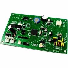
What is the process of etching a circuit board?
After cleaning, the printed circuit layout is transferred onto the copper surface. This can be done using several methods, including photolithography or direct printing. In the photolithography process, the transparent film is placed over the board, and ultraviolet (UV) light is used to expose the copper layer through the film. The areas of copper that are exposed to light will become hardened, while the unexposed areas remain soft. This is followed by a development process that removes the unexposed copper, leaving the desired circuit pattern on the board.
Once the design is transferred, the actual etching process begins. The board is submerged in an etching solution, typically a mixture of ferric chloride or ammonium persulfate. This solution dissolves the copper in the areas that are not protected by the hardened photoresist, effectively removing unwanted copper and leaving only the desired circuit pattern. The etching process requires careful monitoring to ensure uniform results, as over-etching can lead to the removal of essential copper features, while under-etching can leave unwanted copper on the board.
After etching, the board is thoroughly rinsed to remove any residual etching solution and then dried. The next step involves removing the remaining photoresist, which can be done using a solvent that dissolves the resist layer. At this point, the PCB has its copper traces exposed and is ready for additional finishing processes, such as applying a protective coating or solder mask. These coatings help protect the copper from oxidation and improve solderability.
For multi-layer boards or those requiring through-hole components, drilling is necessary to create holes for component leads. These holes may then be plated with copper to ensure electrical connectivity between layers. This plating process involves depositing a thin layer of copper into the drilled holes, typically through an electroplating method, which enhances the circuit board’s overall functionality.


