

RF Boards Used in Mobile Phones
Yes, RF (Radio Frequency) boards are used in many modern technologies that rely on wireless communication. This includes mobile devices, radar systems, GPS units and wireless networking equipment. The ability of RF PCBs to efficiently manage high-frequency signals makes them indispensable in these technologies.
An RF PCB has to perform the same functions as any other PCB, but it must handle extremely fast-moving signals that require the highest level of signal integrity. RF circuits are prone to EMI or electromagnetic interference, so the board must have adequate shielding and impedance matching to avoid loss of signal strength and degradation of the output power. RF circuits also require tight tracing widths and a high degree of precision when routing them through the PCB. In addition, they are a frequent source of heat due to their high-frequency nature, so it is important that the material used for the PCB can dissipate the heat effectively.
rf board are usually made from materials such as FR4, FR3, PTFE, FR-A or ceramic filled PTFE, with the choice typically based on the requirements for electrical performance and cost. Since RF PCBs are so sensitive to the effects of thermal stress, it is essential that the materials be able to endure the soldering process during assembly without suffering from deformation or warping.
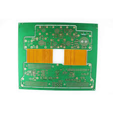
RF Boards Used in Mobile Phones and Radar Systems
Another crucial consideration for RF PCBs is their sensitivity to noise. The RF signal passes through the board as electromagnetic waves, which can be affected by the dielectric material of the layers and the traces. To reduce the risk of noise, RF PCB designers should minimize the length of signal traces and use small components where possible. They should also route them away from digital traces, power planes and other sources of noise.
It is a general principle that digital circuits should be kept away from analog circuits, and this also applies to RF PCBs. This is because the two kinds of circuits operate at different frequencies and have very different characteristics. If they are too close, the digital circuits can cause interference with the analog circuits, resulting in distortion or other problems.
In RF PCB designs, the distance between adjacent features will also play an important role, because these circuits are prone to interacting with each other in unexpected ways. In addition, RF boards must have sufficient shielding to prevent electromagnetic interference from other devices.
During the development process, RF PCBs are prototyped using techniques like TDR and S-parameters testing to check performance and ensure that the design meets all the necessary criteria. Once the PCB is ready for production, it is fabricated using special machinery such as plasms etch technology to create thru-holes with tight tolerances and precise tracing widths.
The RF PCB in a modern cell phone requires multiple antennas to transmit and receive signals. Depending on the technology, there may be as few as 6 or as many as 16 antennas (3G, 4G, 5G, WIFI, GPS, etc). For each antenna, there must be a path that carries the signal from the antenna to the model, and this is referred to as an RF chain.