

printed circuit prototype be used for RF designs
A printed circuit prototype is an early version of a finished product that allows engineers to test and validate their design. A prototype can also serve as a guide for the fabrication and assembly process. This helps ensure that the final product will function as intended and reduces the risk of producing faulty or inefficient products during production.
RF designs are complex and require careful consideration of the electrical properties of printed circuit prototype material, components, and layout. Proper design techniques help reduce parasitic effects and increase efficiency. This includes careful component placement, controlled impedance design, and careful traces routing. It also requires an understanding of physics and the impact of materials on RF circuits.
The choice of substrate material is also important for RF design. Many RF circuits are designed on multilayer boards. This is because the RF signals typically need a good ground reference, which can be accomplished using a coplanar stripline. Single-layer circuit boards are not suitable for RF design because they lack the space needed for a ground plane.
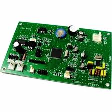
Can a printed circuit prototype be used for RF designs?
A multilayer board is also the preferred option for RF designs because it provides an efficient way to route RF signals. The RF signal layer can be separated from the digital and analog layers, which reduces interferences between them. It is also possible to place a decoupling capacitor between the RF signal layer and the power supply to filter out noise.
Other important considerations in RF design include the selection of components, proper layout techniques, and a good grounding strategy. RF designers must carefully consider the location of all ICs and components to avoid any cross-coupling or feedback loops that can cause instability and loss of performance. RF designers should also take care to choose the right capacitors for decoupling. The optimum choice is one that operates at its self-resonant frequency (SRF) to achieve the best decoupling efficiency.
For RF applications, it is also important to remove the solder mask from RF traces to prevent increased losses due to the higher dielectric constant of the solder mask. It is also a good idea to avoid placing test points on RF traces because this can interrupt the trace’s impedance matching values. Instead, RF traces should be connected to a dedicated ground plane and accessed by using a bridge area.
Lastly, it is important for RF designers to use a CP Differential Pair arrangement. This design technique separates the RF signal layers from each other and eliminates parasitic inductance caused by plated through via holes. This is important because a small inductance can have significant effects on high-frequency signals.
Creating a functional prototype is the first step in the RF circuit development process. Once the prototype is created, it should be thoroughly tested to make sure that it meets all design requirements and functions as expected. This is a critical step because it can save time and money by eliminating the need for a full-scale production run of the final product.


